
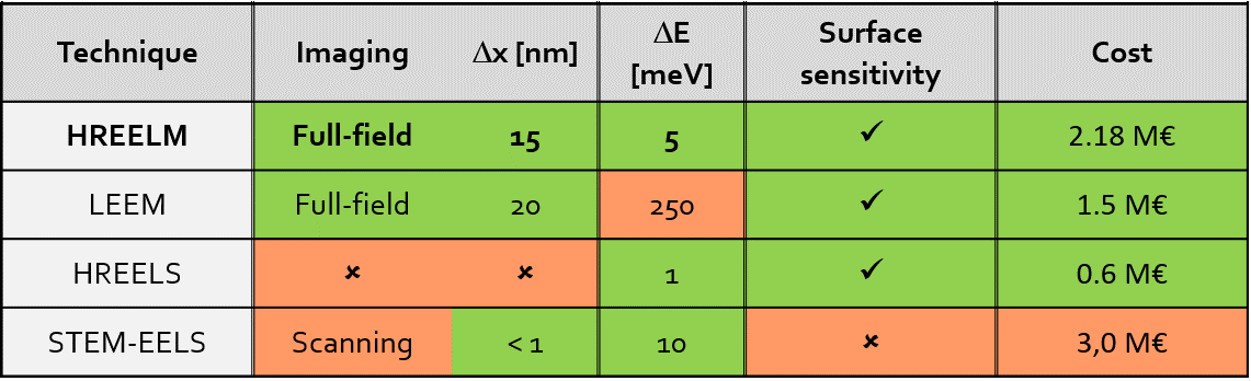
HREELM - High resolution electron energy loss microscopy - 3
The aim
Imaging for the first time the surface vibrational states with nanometric spatial resolution
This will be done by full filed imaging of loss energy electron energy losses in real and reciprocal space at high spatial (15 nm) spectral (5 meV) and wave-vector (40 cm-1) resolutions.

State of the Art
Funding
Le projet SESAME, coordonné par Lionel Amiaud (ISMO), avec Daniel Comparat (LAC) et Nick Barrett (SPEC), a obtenu un financement de 1,1 M€ permettant d’envisager la construction du prototype dans les 3 ans à venir.
The cumulated investment since 2014 is illustrated below

The multidisciplinary nature of the project will contribute to structuring collaborations in the Paris Saclay campus, in the Ile-de-France region and also internationally with both research institutes and industry.

We’d like to thank all of the supporting laboratories, institutes and companies. Here are just a few examples from colleagues and collaborators:

Programme et Equipements Prioritaires de Recherche (PEPR) sur l’Électronique
L’électronique est au cœur des fonctionnalités numériques des produits et services dans nos sociétés et devient un enjeu stratégique faisant l’objet de forts risques de prise de contrôle que ce soit par des industriels étrangers ou d’autres états.
C’est fort de ce constat que le gouvernement a fait de l’électronique un choix prioritaire dans sa stratégie nationale de recherche et de développement technologique et industriel et a notamment confié au CNRS et au CEA le pilotage d’un PEPR visant à générer des innovations pour accélérer la croissance et relocaliser certaines productions en France ou en Europe grâce à des solutions technologiques nouvelles.
Le PEPR Électronique impliquera plus de 60 équipes de recherche (350 scientifiques permanents) du CNRS et de ses partenaires et formera plus de 60 doctorantes et doctorants et 60 post-doctorantes et post-doctorants.
Les thématiques prioritaires du programme sont :
La perception numérique
L’électronique pour la conversion
Les composants pour les télécommunications
L’électronique pour le calcul
Co-pilotes : CNRS / CEA
Budget : 86 millions d’euros

Work Package 4 ELECTRONIQUE POUR LE CALCUL
4.2 Paradigmes de calculs bio-inspirés neuromorphique
· Développement de la synapse artificielle hybride ferroélectrique/memristive
· Capacités d’apprentissage (ferroélectricité) et d’utilisation à long terme (memristor)
· Synapses ferroélectriques à ultrabasse consommation d’énergie
· Réalisation de démonstrateurs avec apprentissage sur puce, associant circuits CMOS et
synapses artificielles
Une thèse financée .
Ferrofutures
Ce projet : “plateForme fERROélectrique pour le calcUl embarqué critique : efficaciTé, peRformancES, adaptibilité” est financé par le PEPR Accélérateur Electronique.

Ferrofutures aims to demonstrate all of the scientific and technical elements required for the value chain of a future French ferroelectronics branch capable of responding to the needs of embedded artificial intelligence (eAI).
The internet of things (IoT) is a major accelerator of a society based on information exchange and requires the deployment of eAI at the edge. Current energy consumption of conventional AI is incompatible with edge applications. Edge AI must satisfy the constraints of frugality, latency, real time operation, exponentially growing data flow and confidentiality. New architectures, capable of local data storage and treatment need to be explored in the light of new emerging technologies.
Amongst them, ferroelectrics offer by far the best energy consumption, allowing access to low-cost non-volatile functionalities, several orders of magnitude more frugal than competing technologies. Since the first publication in 2011 on ferroelectric hafnium dioxide, the field has literally taken off internationally and France possesses the trump cards covering the full value chain.

Building on pioneering work on HZO (HfZrO2) ferroelectric memories, more eco-compatible than the PbZrTiO3 (PZT) predecessors, Ferrofutures will integrate this emergent techonology with innovative circuit and systems architectures for eAI. This Technology-Circuit-System organization will be implemented along two axes:
· Optimization of a ferroelectric component (a FeMFET) with low operating voltage, endurance better than 1012 cycles, non-destructive read, zero imprint, integrated into test arrays and innovative circuits for embedded microcontroller logic;
· Groundbreaking circuit and architecture concepts for vectorial, high throughput (>100Mo/s), data logger computation on the MAD200 test platform, and which will produce a demonstrator chip.
In this way the combined efforts of the Ferrofutures partners will address:
Compact modelling to ensure the convergence of circuit design and technology to long term application perspectives;
Demonstration of x2-x10 energy gain and x8 latency reduction with respect to state of the art high throughput embedded FeRAM data loggers.
Their internationally recognized previous work makes the Ferrofutures partners particularly suited to the collaborative work needed to attain the project aims. The IMS, INL and IM2NP laboratories are the best equipped to realize proofs of concept beyond the international state of the art in compact modelling, design and fabrication of innovative circuits; the expertises of the IRAMIS, LETI and LIST institutes of the CEA in advanced characterization of ferroelectric oxides, of the integration potential of memory technologies and of embedded critical systems are internationally recognized.
We are confident that Ferrofutures will open the way to a French Ferroelectronic branch.
Soleil et MicroElec
Projets ciblés du PEPR Diadem avec Soleil, Greman, ISCR, Leti
Début 01/04/2023

Innovation in functional materials is key to increase the competitiveness of a sustainable, more efficient microelectronic industry in Europe. In the recent years, a new approach targeting accelerated materials discovery has been developed with the high throughput production and screening of material libraries. We propose to extend this high throughput combinatorial approach to multi-layered microelectronics devices whose functional properties depend on both the nature of each constitutive layer and on the interplay between those layers. Improving their performances thus requires optimization of the stack as a whole. Understanding and engineering this complexity through artificial intelligence (AI) assisted combinatorial synthesis / high throughput screening and analysis of heterostructures libraries having systematic and simultaneous variations of key parameters would speed up efficient devices elaboration and generate massive material database resources. To validate this AI assisted high throughput development in the field of microelectronic applications, existing combinatorial synthesis and characterization platforms will be expanded and applied to define the best suited lead-free materials / heterostructures to be integrated in micrometric piezoelectric actuators and nanometric ferroelectric non-volatile memory.
Ferro4EdgeAI
SCALABLE FERROELECTRIC-BASED ACCELERATORS FOR ENERGY EFFICIENT EDGE AI
Horizon Europe CL4 avec Leti, NaMLab, INL, TU Delft, ST Microelectronics, FMC, SynSense
Début 01/01/2024
The Ferro4EdgeAI project will provide an ultra-low power, scalable edge accelerator for artificial intelligence incorporating a memory augmented neural network, based on low cost, high density, multi-level, Back End of Line (BEoL) integrated ferroelectric (FE) technology.
We expect to achieve a 2500x gain in energy-efficiency to break the POPS/W barrier with respect to the state-of-the-art CMOS accelerators and predictions for other emerging technology AI hardware. To do so, five ambitious specific objectives have been selected:
- multi-level functionality in hafnia-based thin films by investigating the optimum trade-off in memory window, film thickness & stability of the ferroelectric state
- low operating voltage for the non-volatile memory and robust multilevel operation of the FeFET-2 for high density logic operations and data storage. A low operating voltage is mandatory for power rating reduction, while robust multilevel operation is essential for analogue in-memory computing at the edge.
- integration and characterization of multi-level, low voltage, FeFET-2 arrays
- definition, design and demonstration of a low power FE AI accelerator suitable for scalable systems integration
- Systems simulation of ultra-low power FE accelerator enhanced edge processing for targeted edge applications of voice and image recognition
ECHOES Edge seCurity witH ferrOelectric dEviceS
ANR avec INL et IM2NP
Début 01/01/2024

Edge-computing is a key solution to sustain the development of data-centric applications in dense networks of sensor nodes. Besides computing efficiency, bringing security solutions is essential to ensure data protection from their collection at the edge’ side to their transmission to the cloud. While edge-security starts to be addressed by the community using cryptography and security primitives such as Physical Unclonable Functions (PUF) or True Random Number Generators (TRNG), secure key storage for cryptography remains sparsely explored since a secured Non-Volatile Memory (NVM) is implicitly assumed. Over the last decade, emerging Ferroelectric NVM (FE-NVM) based on Zr-doped hafnium oxide (HZO) have attracted alot of attention for embedded applications thanks to their excellent compatibility with advanced CMOS nodes, high endurance and ultra-low power consumption as compared to other competing, emerging technologies. Besides Flash replacement, their intrinsic stochastic switching at nanoscale makes them valuable candidates to implement edge-security solutions from secured eNVM arrays to FE-based PUFs and TRNGs. However FE-NVM still suffer from some undesirable effects such as imprint which raises major issues for security applications. Although highly debated in literature, physics behind imprint in HfxZr1-xO2 (HZO) is not elucidated to date and is rarely taken into account when evaluating emerging FE-based circuits. In this context, the goal of ECHOES is to determine whether HZO-based FE NVM can outperform current NVM solutions for edge-security applications by addressing three objectives:
(i) Bring a comprehensive understanding of imprint through advanced characterization and physical modelling: Benefiting from state-of-the-art FE capacitors, ECHOES will combine a wide variety of physical, chemical and electrical characterization techniques to conduct in-depth and complementary analysis to establish detailed correlations between electrical performances (including reliability and imprint) and material properties. The collection of a wide ranging data from devices subjected to various processing or operating conditions will be then leveraged to build a physical model of FE devices based on phase-field modelling that will serve as a unified framework connecting materials and defects properties to imprint at the device level.
(ii) Develop imprint-free FE devices through materials and interface engineering: ECHOES will follow a defect control and engineering strategy based on various interface and electrode engineering approaches such as optimizing FE film thickness, composition, nanostructure and processing conditions thanks to the combination various deposition techniques. We will leverage on this wide exploration space to identify and deploy technological solutions to imprint beyond the current state-of-the-art in order to fulfil specifications for edge-security.
(iii) Demonstrate the efficiency of secured FE storage solutions implementing imprint mitigation strategies at the circuit level: FE memory arrays will be designed at advanced CMOS nodes with laying the ground to the design and evaluation of security primitives. Dedicated FE imprint-aware compact models calibrated on data gathered on micro- to nano-scaled devices will be leveraged to demonstrate the relevance of FE eNVM for edge-security applications. The impact of imprint on circuit performances will be systematically evaluated to provide guidelines at the device level for the fabrication space exploration.
Reaching the aforementioned objectives requires a close scientific collaboration covering the fields of material science, device engineering & modelling and circuit design based on emerging technologies. Thus the project adopts a DTCO (Design-Technology Co-Optimization) approach allowing to evaluate and quantify the individual and synergetic contributions to imprint and to the mitigation strategies.
TPX4
Time and Position sensitive fast piXel detectors for 4D electron spectroscopy
ANR avec LPS, LAC, ISMO
Début 01/02/2024

The aim of TPX4 is to demonstrate the feasibility of two new types of electron spectro-microscopies: Time-Resolved Cathodoluminescence Excitation spectroscopy (TR-CLE) and High-Resolution Low Energy Electron Microscopy (HRLEEM). Both ally extreme spatial, energy, and temporal resolutions needed to tackle current challenges in nanosciences. TPX4 relies on the development and use of a new and unique pixelized direct electron detector combining sub-ns temporal resolution and high flux to achieve both TR-CLE and HRLEEM. This ambitious goal will be explored by a consortium of leading experts in instrumentation development for applications of electron microscopy and spectroscopy.
D3PO
Dopant and Defect Physics for Device Optimization for Hafnium Oxide based Devices
Dopage et physique des défauts pour l'optimisation des propriétés électriques de l’oxyde d’hafnium ferroélectrique
Devices realized with ferroelectric hafnium oxide are silicon compatible, power-efficient, and can be cost-effectively integrated into advanced technology nodes for sensor, nonvolatile memory, logic, and neuromorphic applications. Currently, hafnium-zirconium mixed oxide (HfxZr1-xO2) offers the widest stoichiometry window for fabricating ultrathin ferroelectric films with large remanent polarization. Still, the film requires oxygen vacancies (VO) to stabilize the ferroelectric phase and has reliability issues. VO concentration is difficult to control and can affect electrical properties such as polarization stability, jeopardizing the prospect of hafnia-based memory and low-power logic.
An alternative could be to start from stoichiometric, quasi-vacancy-free hafnia and use suitable dopants to optimize the ferroelectric properties. This would have the significant advantage of being more reproducible than the rather uncontrolled generation of VO in HfxZr1-xO2.
We will explore this possibility by studying the atomic and electronic structure of selectively and controllably doped hafnia using ab initio calculations and phase-field simulations to describe the influence of the dopant modulated atomic and electronic structure on the ferroelectric properties. A range of dopants, concentrations, and process conditions will be considered to provide an initial assessment of the correlations between dopant chemistry and the ferroelectric properties.
The chosen materials will be characterized on large area capacitors and optimized by successive simulation, processing, and characterization iterations. Then they will be integrated into scaled capacitor arrays to provide statistically significant results on ferroelectric capacitor performance. At a fundamental level, D3PO will give a better understanding of the influence of dopants on local chemistry, electronic structure, phase composition, and their effects on material and ferroelectric parameters, including recrystallization temperature and remanent polarization.
We will then elaborate physical models based on real devices, using parameters obtained from ab initio simulations and structural and electrical characterization to predict, through statistical analysis, key metrics such as wake-up, endurance, retention, leakage, and breakdown using vacancy-free doped hafnia.

The project is a Franco-German collaboration between the CEA, NaMLAb (Dresden) and the Technische Hochschule München, jointly funded by the ANR and the DFG.
Collaboration STMicroelectronics
Thèse CIFRE
Début 01/11/2022
A STMicroelectronics, les mémoires sont co-intégrées avec les transistors au sein d’une même puce. Ce type de fonctionnalité, qu’on appelle ‘mémoire embarquée’, est utilisé pour la fabrication de microcontrôleurs. Or l’HfO2 est largement utilisé pour la fabrication des puces où il sert d’oxyde de grille pour les dernières technologies. Il a été montré en 2011 [Böscke2011, Müller2012] que la phase orthorhombique d’HfO2 est ferroélectrique à température ambiante. On voit donc l’intérêt de ce matériau qui devrait permettre de co-intégrer des transistors CMOS digitaux et des transistors ferroélectriques au sein d’une même puce.
L’étape suivante est de comprendre comment stabiliser la phase ferroélectrique avec l’architecture et les températures de l’intégration « Gate first » utilisée à STMicroelectronics. Une étude thermodynamique et cinétique est nécessaire et les effets des différentes étapes utilisées (budget thermique, rampes de température, architecture, contraintes) doivent être quantifiés. L’objectif est le contrôle du champ électrique par la polarité afin d’avoir un changement suffisant de tension de seuil des transistors entre l’état « 0 » et l’état « 1 », typiquement d’environ 0.5 V. Le champ électrique interne est aussi déterminé par des charges qui peuvent se piéger dans ces matériaux, dans l’oxyde de silicium sur lequel il repose, ou aux interfaces avec le SiO2 et l’électrode.
Le principe de la spectroscopie des photoélectrons consiste à analyser l’énergie cinétique d’électrons excités par des rayons X, et cette énergie cinétique va dépendre aussi des variations de potentiel, donc du champ électrique, dans le matériau. On envisage l’utilisation de la technique pour la mesure de variations de potentiel.
Les matériaux seront élaborés dans l’unité de production 300mm de STMicroelectronics. STMicroelectronics est impliqué dans la proposition du projet européen Phaistos 2.0. Si celui-ci est accepté l’étudiant pourra profiter des échanges avec différents laboratoires européens spécialisés dans les matériaux ferroélectriques, comme le NaMLab (Dresde). Les échantillons seront ensuite caractérisés par les campagnes d’analyse par la spectroscopie des photoélectrons.
Les analyses XPS en laboratoire seront menées au centre CEA Saclay à l’UMR 3860 SPEC CNRS CEA
Nous utiliserons la spectroscopie des photoélectrons avec les rayons X (HAXPES) durs avec le rayonnement synchrotron afin d’analyser le champ électrique interne dans les structures avec une électrode supérieure plus réaliste entre 10-20 nm. Plusieurs synchrotrons sont envisagés, en priorité le synchrotron Soleil et Petra-III, mais aussi des synchrotrons SPring-8 (Japon) et NSLS-II (Brookhaven, USA). Les expériences operando pour quantifier le champ interne en fonction de la polarisation ferroélectrique seront faites avec des empilements microstructurés dédiés aux expériences HAXPES.
En complément aux analyses avec le rayonnement synchrotron, la thèse utilisera le système de HAXPES en laboratoire disponible sur la PFNC à Grenoble (collaboration Olivier Renault). La HAXPES en laboratoire est moins bien résolu énergétiquement et fournit une intensité plus faible qu’au synchrotron mais l’avantage significatif d’être plus facilement et plus rapidement disponible que les expériences synchrotrons suspendus à l’évaluation des comités de programme.
Enfin, nous comparerons les résultats expérimentaux avec les caractérisations électriques et des calculs modèles basés sur l’équation de Poisson en une dimension, utilisant une approximation de Thomas-Fermi [Catrou2018].
Les résultats expérimentaux permettront d’affiner un modèle physique fiable du champ interne, pour l’optimisation du process de la technologie FeFET « gate first ».
Le travail scientifique qui sera effectué durant cette thèse servira le développement d’une technologie FDSOI embarquant une mémoire avec mise en production potentielle d’ici 3 à 5 ans. L’identification des matériaux impliquera également une démarche de développement durable.
[Böscke2011] Böscke, Müller, Bräuhaus, Schröder, Böttger. Ferroelectricity in hafnium oxide thin films. Appl. Phys. Lett. 2011, 99, 102903.
[Müller2012] Müller, Johannes, et al. "Ferroelectricity in simple binary ZrO2 and HfO2." Nano letters 12.8 (2012): 4318-4323.
[Catrou2018] P. Catrou et al., Phys. Rev. B 98, 115402 (2018)
BePolar
Beyond polar dead-layers and leakage in BST-based varactors for NFC and 5G telecommunications
Emerging communication technologies like 5G or Near Field Communication call for voltage tunable ferroelectric (FE) film capacitors to work at higher frequencies or lower voltage, thus requiring the reduction of the FE thickness. Unfortunately, two interface-related phenomena, the FE “dead layer” and leakage current, impede this evolution. Recent encouraging ab initio calculations showed the importance of the chemical bonding, polar discontinuity and distortion mismatch at electrode/FE perovskite interfaces for polarization stabilization and Schottky barrier height (SBH) adjustment. A systematic interface engineering using Combinatorial Pulsed Laser Deposition will chemically modulate electrode/(Ba,Sr)TiO3 interfaces of industrial capacitors. Advanced spectroscopy and microscopy methods coupled with first-principles calculations will help to understand the chemical, structural and electronic mechanisms controlling the SBH and FE polarization at the interface. TRL 6 industrial prototype varactors with the optimized interfaces will be tested against 5G and NFC specifications.
The deployment of 5G technology has raised serious technological issues of energy consumption, reception quality and call failure rate. All three can be minimized by continuouslyadjusting the antenna impedance as close as possible to 50 ohms. An impedance matching scheme is also necessary for Near Field Communications (NFC) technology to allow reliable and energy efficient contactless communications (e.g. for keyless cars, card or phone payments, Internet of Things…) whatever the ambiant transmission conditions. To answer these 5G and NFC needs, a voltage controllable impedance matching circuit with a highly tunable capacitance (a.k.a. varactors) is required. In particular, at least a factor 5 variation (tuning ratio t = Cmax/Cmin>5) and low dielectric losses (inverse quality factor Q = 1/tan) at GHz frequencies are necessary to preserve potential energy gain and a small footprint. Among the various tunable technologies existing on the market (diode based varicaps, high mobility transistors pHEMTs, integrated CMOS transistor-switched capacitors…), voltage tunable ferroelectric (FE) capacitors fullfill tunability and loss requirements and have the smallest footprint [1,2,3]. Indeed, the relative dielectric permittivity er(E) of a FE has a large electric field dependence (Fig. 1) [1].

Permittivity and dielectric losses vs electric field in Pt/BST (240nm)/Pt capacitors (STMicroelectronics Tours) [4]
In order to maintain low dielectric losses at microwave frequencies and retain a high dielectric permittivity, FE materials are usually used in the paraelectric phase, i.e. above their Curie temperature, TC. The perovskite solid solution Ba1-xSrxTiO3 (BST) is the most widely used FE in current varactors because of its excellent tunability/losses compromise associated with an easily adjustable TC (via the Ba/Sr ratio), leading to far better quality factors than competing technologies. STMicroelectronics (ST) uses metal/BST/metal parallel plate capacitors to continuously match antenna impedance in 4G cell phones (Q > 35 at 2.7 GHz), optimizing its radiation properties and saving energy [5].
Financement : ANR (PRCE) 2020
Partenaires : GREMAN (Tours), ST Microelectronics (Tours), CEMES (Toulouse)
[1] A.K. Tagantsev et al. Journ. of Electroc. 11, 5(2003) https://doi.org/10.1023/B:JECR.0000015661.81386.e6
[2] P. Bao et al., J. Phys. D: Appl. Phys. 41, 063001 (2008) https://doi.org/10.1088/0022-3727/41/6/063001
[3] M. Tiggelman et al., trans. Elec. Dev., 56, 2128 (2009)
[4] E. Bouyssou et al., ECS Transactions, 61, 155 (2014) https://iopscience.iop.org/article/10.1149/06106.0155ecst/meta
[5] https://www.st.com/resource/en/datasheet/stptic-27c4.pdf
S. Gonzalez PhD thesis https://hal.archives-ouvertes.fr/tel-01560333v1
GO-FERRO
The aim of this project is to understand the underlying physics of the interface between ferroelectric HfZrO2 and Ga2O3 with a view to the implementation of such a heterostructure in power electronics.
Ga2O3 belongs to the family of ultra wide band gap semiconductors with potentially unrivalled performance thanks to breakdown fields. Ferroelectric materials have two states of opposite electric polarization, switchable by an applied electric field. We propose to study the physical properties resulting from the insertion of a thin ferroelectric film adjacent to Ga2O3 layer.
The robust nature of the FE polarization means that the internal bias can be switched by a simple voltage pulse, reducing leakage and making devices suitable for high-autonomy power switches.
The material of choice is the CMOS-compatible ferroelectric HfZrO2.
We will use advanced photoelectron spectroscopy techniques including synchrotron radiation induced Hard X-ray PhotoElectronSpectroscopy, Photoemission Electron Microscopy and laboratory based X-ray Photoelectron Spectroscopy to understand the coupling between ferroelectric polarization and the Ga2O3 electronic structure.

We propose to use the ferroelectric polarization to overcome the usual depletion mode of Ga2O3 MOSFETs. The internal voltage due to the ferroelectric polarization allows to tune Vth in the MOSFET, thus at 0 V the channel can be ON or OFF.
Financement : Air Force Office of Scientific Research (AFOSR) 2020
HREELM - High resolution electron energy loss microscopy - 3


Un microscope à perte d'énergie d’électrons à haute résolution spectrale (HREELM) pour étudier les états vibrationnels des surfaces à l'échelle nanométrique. L’objectif du projet est d’optimiser le système de détection/manipulateur hautes résolutions.
Détecteur Timepix4, soft de contrôle et d’acquisition, manipulateur de précision
Financement : Programme Transverse de Compétence - Instrumentation et Détection (PTC-ID)
L’objectif ultime de notre projet est la réalisation d’un prototype d’un nouveau microscope pour les études de surface : un microscope à haute résolution des pertes d’énergie d’électrons (HREELM).
Financement : Projet innovation NanoSaclay
Gun for a high resolution electron energy loss microscope
Combiner nano-structuration de surface, microscopie plein champ et diagnostic spectroscopique : Le but du projet HREELM (High Resolution Electron Energy Loss Microscope) est de combiner une nouvelle source d'électrons hautement monochromatique du Laboratoire Aimé Cotton (LAC) avec les expériences de lithographie chimique contrôlée par électrons de l'Institut des Sciences Moléculaires d'Orsay (ISMO), et avec un microscope électronique spectroscopique plein champ et à haute résolution (Université de Mayence, JGU ; SPEC, CEA). Cette combinaison unique permettra la production et l’utilisation d’un faisceau d'électrons monoénergétiques (~1 meV), de très faible énergie (0-20 eV) et collimaté pour la structuration de surfaces à l'échelle nanométrique et comme outil de diagnostic. Son implémentation sur un nouveau microscope spectroscopique à champ complet, avec une haute résolution spatiale, énergétique, d'impulsion et temporelle (20 nm, peu de meV, 0,003 Å-1 et 150 ps, respectivement), ouvrira également la voie vers l'imagerie spectroscopique à haute résolution des états vibrationnels de surface
3εFerro :
Energy Efficient Embedded Non-volatile Memory & Logic based on Ferroelectric Hf(Zr)O2
1T-1C
Interface characterization & charge injection
Integration of La doped HZO into final 16kbit 1T-1C FeRAM array demonstrator.
Si:HfO2 films have shown much better device-to-device and die-to-die variability than HZO films. Integration into final demonstrator (3eFERRO++)
Zero bitfail has been recorded in the 16kbit 1T-1C array of the 600 nm. The Full ‘0’ and Full ‘1’ states are read after write operations adopting pulses of 2 µs width at 4.8 V. The test vehicle allows to address and read the individual bitcells. Patterns like the 3eFERRO logo can thus be stored in the array.
FeFETs
Gate stacks with different ferroelectric/dielectric bilayers have provided input for the fabrication of the proof-of-concept NC-FeFET.
p-Ge/HZO/TiN and n-Ge/HZO/TiN stacks for exploring the potential benefits of Ge channel structures.
LiM
FRAM structures : 2T-nC, ternary content addressable memory (TCAM) and pseudo-FeFET.
Digital image filter design, implementing HZO based FeFET logic
First results of circuit & system-level benchmarking platform

33 publications in scientific journals, 10+ under preparation
77 presentations at conferences and workshops
5 workshops organized + session DATE 2022
5 issues of the 3eFERRO newsletter
12 PhD theses linked to project
Funding : This project has received funding from the European Union’s Horizon 2020 research and innovation programme under grant agreement No 780302.
MesoXcope
L'objectif de ce projet est d'apporter une contribution révolutionnaire à la recherche fondamentale en utilisant la spectromicroscopie de rayons X sur des surfaces et des interfaces de matériaux multiferroïques pour de nouvelles technologies de l'énergie.
Installation de l'instrument en avril 2013
Financements : SESAME, le Triangle de la Physique, l'Université de Cergy Pontoise, l'Ecole Centrale de Paris, l'Institut Peter Grünberg (Jülich, Allemagne), l'IRAMIS (CEA)