
High resolution spectroscopy is necessary to untangle the electronic structure. Thus, experimental tools which can contribute to a full understanding of the surface and near surface electronic and chemical structure are desirable, if possible with spatial resolution suitable for investigating individual domains or even phenomena localized at domain walls.
Direct experimental data on the electronic structure of a FE next to an electrode is scarce due to the intrinsic difficulties of probing a buried interface. Photoelectron spectroscopy techniques are ideally suited since they reveal both electronic and chemical structure and the nanometric depth sensitivity may be tuned to the buried interface. To do these studies, the key is the combination of high quality sample preparation with state of the art experimental techniques to measure atomic, chemical and electronic structure.
Photoelectron spectroscopy provides information on the initial state of the electron in the material, thus we can measure the chemical and electronic structure as well as the sample work function.
Photoelectron emission microscopy (PEEM) allows photoelectron spectroscopy with sub-micron spatial resolution. It can be used, for example, to perform domain polarization recognition at the surface of single crystal samples.
Photoemission
Photoemission electron microscopy (PEEM) allows imaging the local chemistry, band structure and photoemission threshold or work function with spatial resolution of ~ 50 nm. In the laboratory we use Hg UV lamp with peak emission at ~ 5 eV and a He I/II discharge lamp from FOCUS GmbH providing photons at 21.2 and 40.8 eV. A focusing mirror reduces the spot size to ~ 300 mm allowing faster image optimization and acquisition.
At the synchrotron we benefit in addition from the high intensity, tunable X-raystypically in the region 100-1000 eV.
Deduce the initial state of electron from photoelectron energy and angle → chemistry & electronic structure

Surface sensitive: ~ first few nanometers

Photoemission Spectroscopy (XPS,HAXPES)
X-ray photoelectron spectroscopy (XPS) using an Al Ka source (photon energy 1486.7 eV) is sensitive to local surface chemistry and the electronic structure with a typical probing depth of a few nm.
Hard x-ray photoelectron spectroscopy (HAXPES) is a powerful tool to study local chemical changes at buried interfaces under more realistic electrodes. Hard x-rays (5–10 keV) increase the inelastic mean free path (IMFP) for the same core level electrons and, hence, the probing depth by up to an order of magnitude.

Photoemission electron Microscopy (PEEM)
Microscopy of the surface with photoemission. The work function can be deduced at each pixels of an area on the surface of a material.

Low energy electron microscopy (LEEM) maps the surface electrostatic potential, a sort of complement to the work function mapping by PEEM.
Low Energy Electron Microscopy (LEEM)
Electrons at very low energies are repelled by the surface potential of the material. It’s the Mirror Electron Microscopy mode (MEM). Surface potential observation at the transition between MEM and LEEM.

In diffraction mode, micro-LEED is possible to deduce the in plane lattice parameters and the surface crystallography quality.
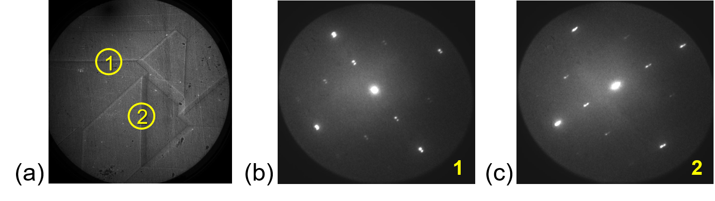
CaTiO3 LEED on ferroelastic domain walls
Synchrotron radiation broadens considerably the experimental possibilities of photoelectron spectroscopy thanks to the tunable, high intensity radiation.
